> It would've been interesting to see an EMI/C report.
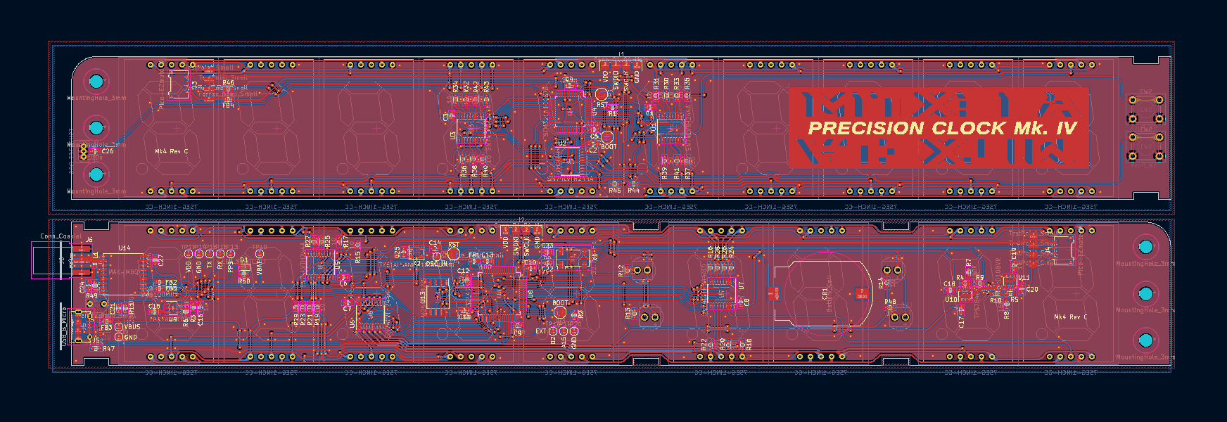
It's a two layer board with no attempts made to keep loop areas small, it's going to be bad. Most of what I read of this seems fine at a glance but that part about EMI sticks out as complete nonsense.
Edit: I have nothing against it being a two layer stackup as part of the art of it, I however don't like that they're also claiming that it's designed to have extremely low radiated emissions while doing so.
That is not correct, with a charitable reading of the text. Which is not to say it’ll have good EMI characteristics - you never really know until you get it tested.
> Artificially confining ourselves to two layers is exactly the kind of challenge I am wont to be engulfed by. The trick, if you want the board to work well, is to work on only one layer, and keep almost the entirety of the other layer as ground. It is almost always possible to do this, if you're willing to put in enough thought. I rather find that designing circuit boards is a lot like Tetris, and once I'm in the swing of it I can route things for hours on end. It can become a multi-day trance, with dreams of signal integrity and current loop area.
Though on this subject:
> In contrast, said this one PCB designer, a thin track has a higher inductance, so if you make your power supply lines thin, you'll get a free bit of extra filtering.
Inductance in your power supply lines is bad, but I don’t have time to get into it right now.
I didn't see that bit, but the layout image[0] shows very large cuts in the ground plane with traces running right over the middle of them, especially between U8 and U7. There's plenty of space here to add some ground traces between them, but that hasn't been done.
> you never really know until you get it tested.
I suspect they haven't given the lack of a CE marking on the board.
As an aside that bothers me a bit given that they say they sold 1000 of the last version, which would easily cover the cost of the (legally required) testing. Normally I'm of the opinion that it's fine to ignore it for some obscure hobby product where the cost of testing would be higher than any expected profits, but in this case they have the money from previous versions of the same product.
For just the EU EMCD and for a simple device like this there's labs out there that will charge as little as $1000. You can technically also do things yourself although I don't know the exact legal requirements off the top of my head.
You can 100% do it yourself, though I think the fact that it has GPS makes it a bit of a weird area because it starts to become a radio even if it's not an intentional transmitter (I've had people who work at EMC test labs tell me they don't understand WTF the standards are actually supposed to mean for GNSS kit). But for a regular electronic gadget you don't need a lab with the right certificates or anything, it's just a declaration on your own liability that you think it meets the required standards. If you're happy to do this yourself and that gives you enough confidence to sign it off, you can. (And in practice the regulators don't really come knocking for small stuff like this unless it's somehow doing something catastrophically bad)
Around here (US East Coast), a day of testing at an FCC-accredited lab for self-certification (so without the lab having to do the TCF or their own documentation) of a small device without unusual IO or power requirements costs between USD $1K-$4K.
>Inductance in your power supply lines is bad, but I don’t have time to get into it right now.
Not always. You want to have appropriate nearby bypass capacitance, but it's common to filter power lines by deliberately adding inductance into them (this also requires care to avoid setting up resonances, but a thin trace will also add some resistance which helps with that). Either way it's not likely to make a detectable difference on this kind of PCB anyway.
A case would probably have it back in spec, if its even out of spec on it's own. The energy is going to be so tiny in those high frequency waves because it's just signal and clock. Never mind that they are still pretty low frequency and those traces are going to be awful emitters in that range.
The highest energy part of the device is going to be the LEDs, which are switching well below the bottom of the standard EMI compliance range (10Mhz).
MCU outputs can be nasty with their high switching speeds. Every STM32 has some slew rate limiting as far as I know, but I looked at their code on GitHub and they're explicitly turning it off for most pins so I assume it's not an option for their driver ICs for some reason.
It's a two layer board with no attempts made to keep loop areas small, it's going to be bad. Most of what I read of this seems fine at a glance but that part about EMI sticks out as complete nonsense.
Edit: I have nothing against it being a two layer stackup as part of the art of it, I however don't like that they're also claiming that it's designed to have extremely low radiated emissions while doing so.